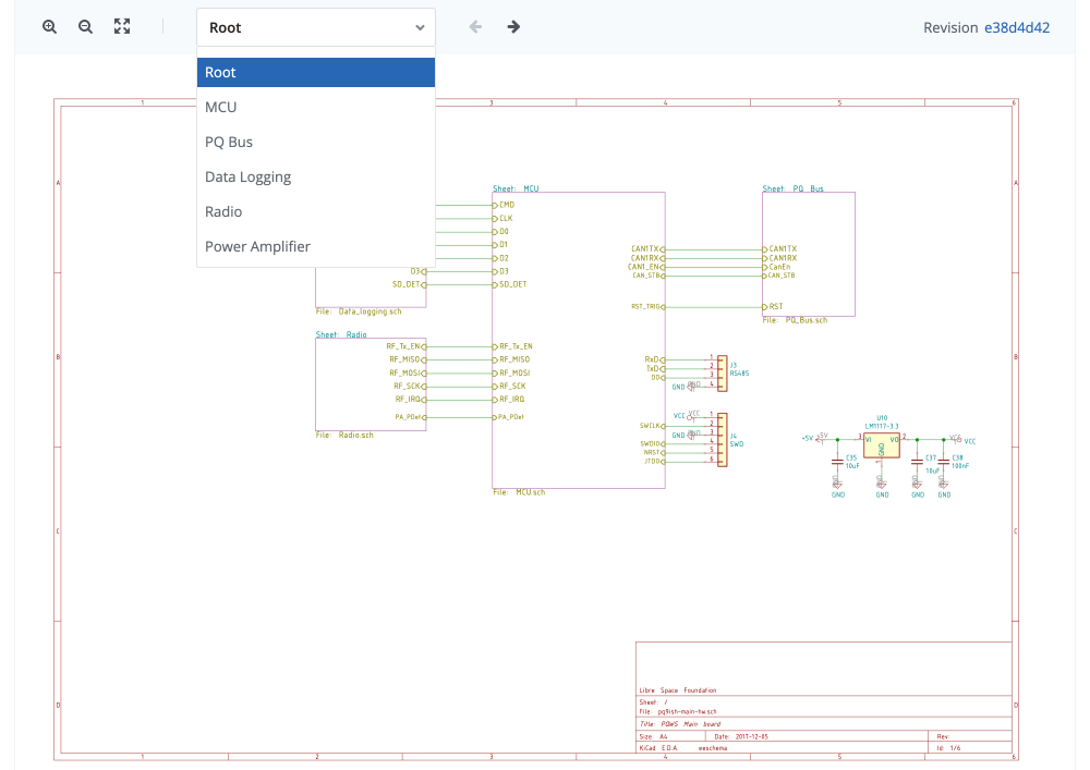
Online Kicad Schematic Viewer
Rotating and panning around features help to inspect details. Additionally, we offer contracted feature development options.
Pic_programmer.kicad_pcb demo will not load Layout KiCad.info Forums

Automation systems and integration — product data representation and exchange.it is known informally as step, which stands for standard for the exchange of product model data.

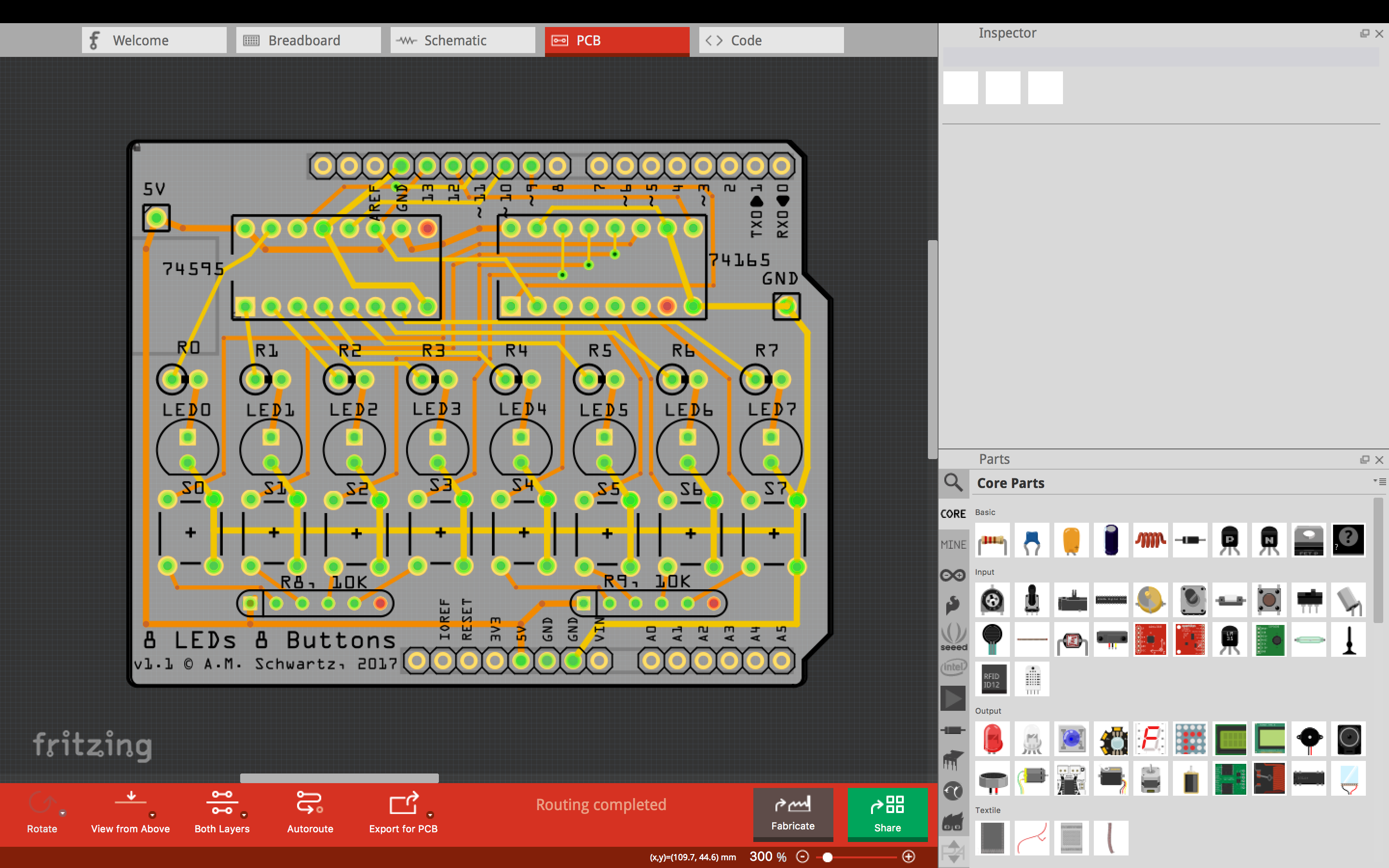
Online kicad schematic viewer. This window is the launchpad for the other kicad apps, like eeschema (the schematic editor) and pcbnew (the layout editor). In pcbnew, click on the view menu, and then choose the 3d viewer. Other than the source code itself there are some other distibruted elements that make up the full kicad package:
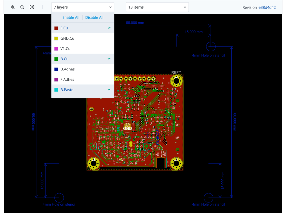
With the kicad project maintaining its own online repository, and new plugins arriving all the time. Copper pour solid region design rule check footprint attributes design manager import changes panelize layout pcb without schematic pcb preview 3d model manager pcb information pcb modules. 59 its official title is:
If you do not have access to any of the above applications, the easiest way to view the circuit board design contained within a brd file is to upload it to altium 365 viewer, a free, online. Ultra librarian provides schematic symbols for schematic capture, pcb footprints for pcb layout and 3d models for the 3d viewer. It has a 3d viewer that you can use to inspect your design on canvas.
Kicad is a free software suite for electronic design automation. A cross platform and open source electronics design automation suite, kicad eda includes schematic capture, pcb layout, and a 3d viewer for electronics engineers. Kicad project manager *.pro eschema schematic editor (both schematic and component) *.sch, *.lib, *.net cvpcb footprint selector *.net pcbnew circuit board editor *.kicad_pcb gerb view gerber viewer all the usual gerber bitmap2component convert bitmap images to components or footprints *.lib, *.kicad_mod, *.kicad_wks pcb calculator
Schematic capture, printed circuit board layout, gerber file viewer, solid model viewer, and much more. Here you can draw schematics for the design you choose. A keen look at this 2n3055 based variable voltage current power supply circuit using transistor 2n3055 reveals that it’s actually only an ordinary stabilized power supply circuit, however it yet still provides you with the proposed features very efficiently.the voltage variations are made by using the preset p2, through a feedback.
If you do not have access to any of the above applications, the easiest way to view the circuit board schematic contained within an sch file is to upload it to altium 365 viewer, a free, online cad file viewer (web). Kicad is a full feature electronics development application for the design and manufacture of electronics that runs natively on windows, osx, and linux. It was developed in yorkshire, england by labcenter electronics ltd and is available in english, french, spanish.
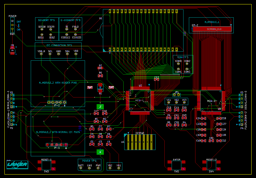
The serious packages are geda and kicad. The wizard walks you through the import process and handles both the schematic and pcb parts of the project, as well as managing the relationship between them. You can see the main kicad window in figure 5.2.
This free cad program allows you to modify the appearance of the board. Schematics, pcb layout and 3d visualization provides a interactive cad experience with no downloads or installations required. The netlist file, generated from the schematic is usually missing the footprints that correspond to the various components.
Add the parts to the cart, and then submit the payment. The wizard is a quick and simple way to convert kicad design files to altium designer files. An interactive 3d view helps to instantly inspect your design easier than with a 2d display.
The programs handle schematic capture and pcb layout with gerber output. Export schematic export bom export. It includes a schematic editor for creating and editing schematic designs, a pcb editor for making professional pcb layouts with up to 32 copper layers, and a 3d viewer which can be used to inspect the design in a 3d form.
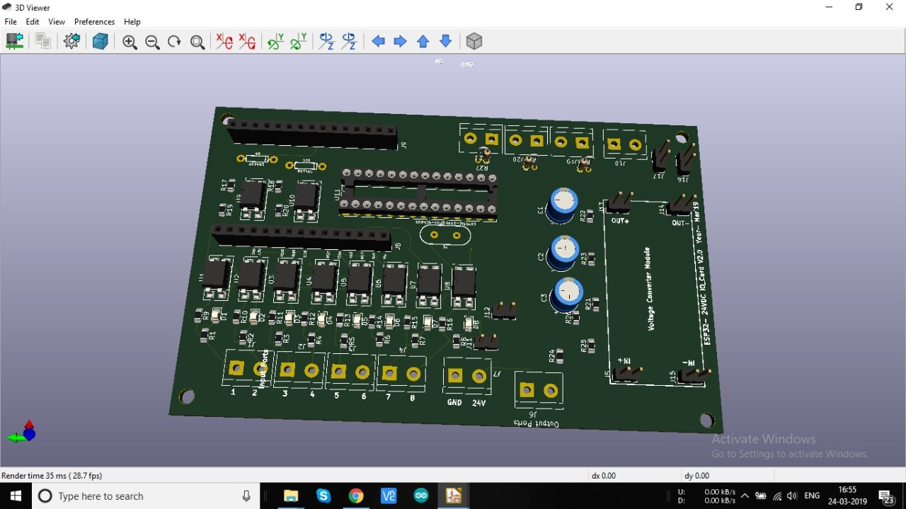
A large library of 3d models is offered. Kicad comes with an excellent integrated environment for schematic entry and pcb layout design. It also provides an array of useful tools that allow developers to create 3d views of the pcb, its components, gerber files, artworks, and bill of materials.
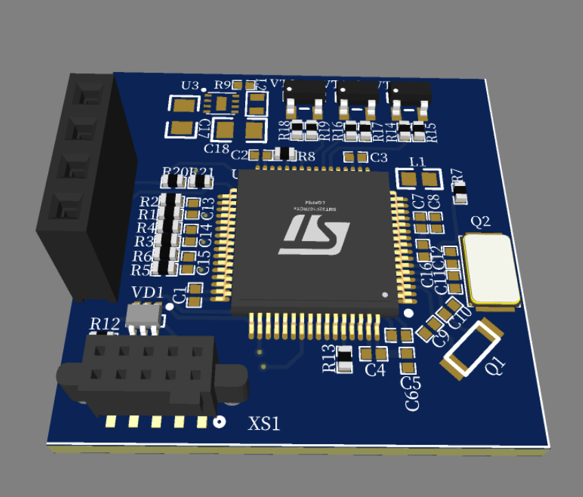
It would also be nice if the 3d viewer stopped saying. Kicad’s integrated 3d viewer helps you view your pcb designs in 3d. If you like the freedom and flexibility of kicad’s open source pcb software solutions you are going to love how we support it.
When you are designing your printed circuit board schematic, there are a few basic concepts you should keep in mind, regardless of how. The 3d viewer can be launched by selecting 3d viewer from an active project. The free, open source software allows you to create pcb layouts and schematics, and even includes a 3d viewer.
During this intermediate process the association of components with footprints is performed. Create designs without limit, make professional pcb layouts, and inspect designs in an interactive canvas with kicad eda. We provide private issue reporting, rapid fixes and online remote desktop support.
I did that for the voltage sensor) it is very satisfying to inspect your work in full 3d after hours of nitpicking and screwing around with traces and placement. Import image import dxf import altium designer import eagle import kicad. They are very sufficient except my professor requires the .out file generated by pspice, so i still have to use that.
This application supports a wide array of tools. Lay out boards more quickly They include a schematic capture, a simulator, a waveform viewer, and a pcb layout tool.
In kicad, cvpcb is used to create this association and a file named *.cmp is. The 3d viewer will show you a. You can open an sch file in a variety of pcb design applications, including:
They are each a collection of programs that work well together (like orcad); Altium designer includes the capability to import kicad ® files through the import wizard. A new schematic window appears with a blank space for working.
This is the first step to achieving your design. Up to 32 copper layers; It features an integrated environment for schematic capture and pcb layout design.
The tool contains a large library of 3d models. Finish the schematic and pcb design at easyeda. It facilitates the design of schematics for electronic circuits and their conversion to pcb designs.
The proteus design suite is a proprietary software tool suite used primarily for electronic design automation.the software is used mainly by electronic design engineers and technicians to create schematics and electronic prints for manufacturing printed circuit boards. Consequently an intermediate stage is necessary. A new experience to help make your design a snap.
Altium 365 viewer is a simple and convenient way to view and share electronic designs through your browser. Never search the internet for verified libraries again, you now have a source with. With a schematic editor, you will be able to design your schematic for the pcb.
KiCAD experience Projects of Jaanus Kalde

Design of the layout Layout KiCad.info Forums
kicadboardeditorpcb Build Electronic Circuits

Download Suite Kicad PCB layout editor Linux Windows e MAC Gratuito Kicad é um programa op

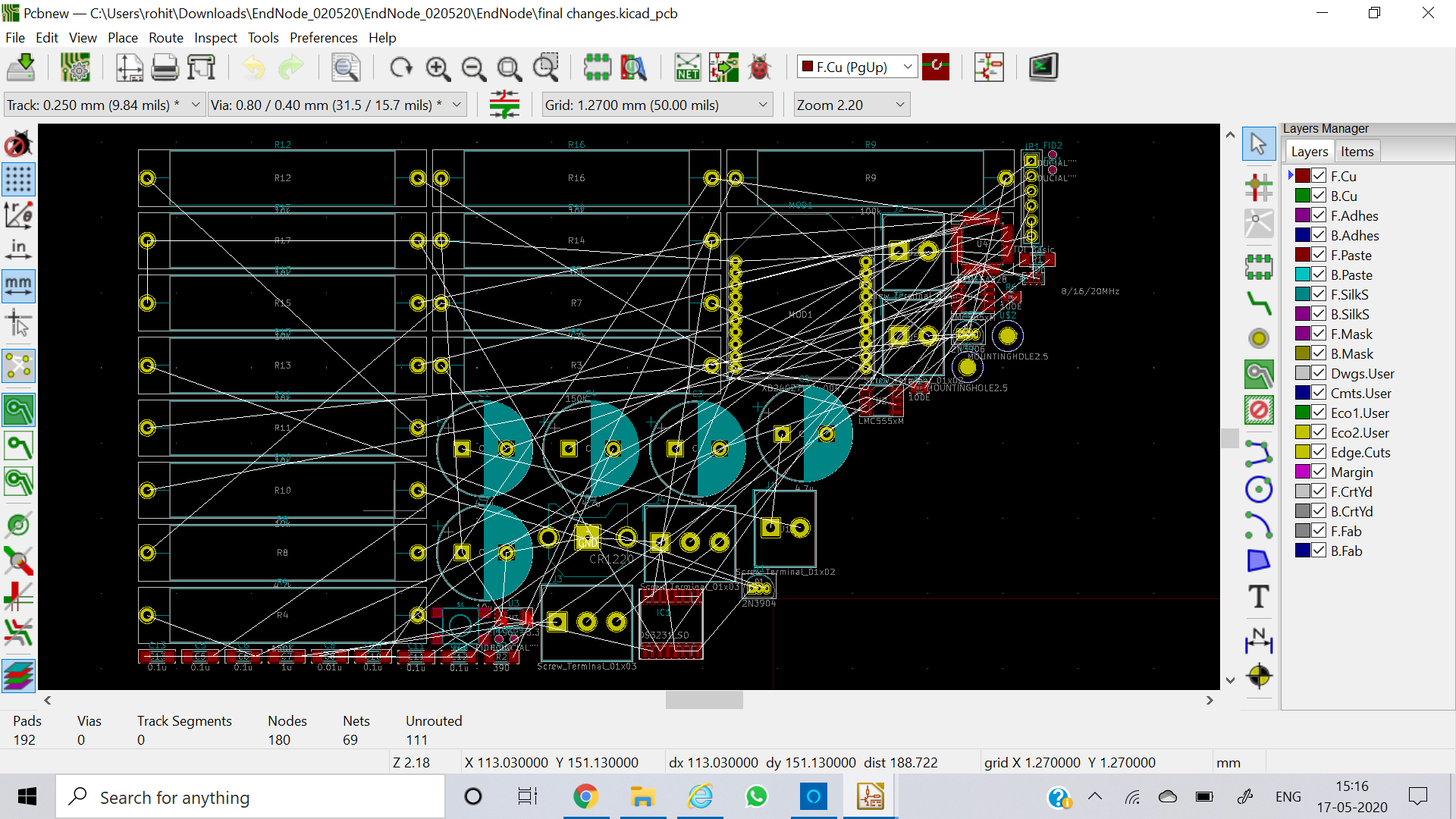
Kicad Pcb Viewer Online PCB Designs
Kicad Pcb Viewer Online PCB Designs
KiCad + PCB Library Expert Software KiCad.info Forums

PCB Designing Software Installation (KiCAD in English) YouTube

Visual version control for KiCad is officially released CADLAB.io
KiCad 5.1.5 Free Download

KiCad CERN’s contribution to Free/Open PCB design Dangerous Prototypes

Kicad 3d Viewer No Components Pcb Circuits
KICAD PCB layout 3 YouTube

Top 8 Best Free PCB Design Software An Ultimate 2020 Updated Guide

STEP Export from PCB 3D Models KiCad.info Forums

Kicad Pcb Viewer Online PCB Designs
Visual version control for KiCad is officially released CADLAB.io
Kicad Pcb Viewer Online PCB Designs
Kicad main components Kicad Like a Pro
